By Hamza Faisal
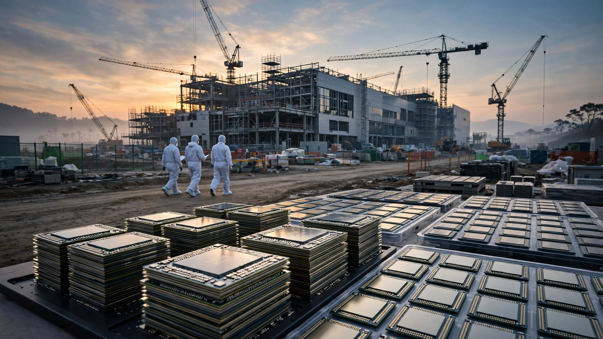
Samsung Electronics has broken ground on a $34 billion advanced chip-packaging hub in South Korea, betting that the artificial intelligence boom will keep demand for high-bandwidth memory outrunning supply for years to come.
The ceremony took place on Thursday at Samsung's Onyang campus in Asan, South Chungcheong Province, with South Korean President Lee Jae Myung and Samsung Electronics Chairman Lee Jae-yong both in attendance. The project is the first to break ground under the government's flagship industrial megaproject initiative, unveiled in late June to build new growth engines in semiconductors, AI data centres and physical AI.
A $34 billion bet on AI memory
The total investment comes to 46 trillion won, or roughly $34 billion. Samsung will spend 6 trillion won building the advanced packaging fab itself, followed by a further 40 trillion won in phased investment in advanced equipment. The plan calls for five high-bandwidth memory packaging lines, and will expand the campus's total floor area from 270,000 to 420,000 square metres.
The new three-storey plant will house around 31,000 square metres of clean-room space and is set to produce seventh-generation HBM4E chips, the next generation of the high-bandwidth memory that sits beside AI accelerators in data centres. Demand for that memory has surged as companies race to build AI infrastructure, straining global supplies and pushing prices higher.
Samsung's semiconductor chief, Jun Young-hyun, outlined a target of June 2028 for the new production line to begin operations, about a year ahead of the original schedule. Samsung moved construction of the line, known as Onyang Line 5, forward to meet demand for AI server memory, and foundational work is already under way.
A year ahead of schedule
The Onyang campus began operations in 1991 as a semiconductor assembly and testing facility, handling the final stages of chip production for general-purpose semiconductors. The new investment will transform it into an advanced packaging hub for high-performance AI chips, including HBM — the heart of the AI semiconductor supply chain.
Packaging has become one of the most contested battlegrounds in the chip industry. As AI accelerators grow more powerful, the way memory chips are stacked and bonded to processors matters as much as the transistors themselves, and the companies that control advanced packaging capacity can shape who gets served first when supply runs short.
Samsung currently operates packaging factories at both Onyang and Cheonan. The company plans to invest a total of 60 trillion won in the Chungcheong region, including the Onyang Line 5 project.
Seoul's industrial push beyond the capital
Two other projects broke ground alongside Samsung's fab on Thursday: an advanced display production line in Asan and a high-performance substrate manufacturing facility for AI servers in Sejong, where Samsung Electro-Mechanics plans to invest 8 trillion won in production lines for advanced semiconductor packaging substrates for GPUs and CPUs.
President Lee said the government would take responsibility for permits, power and water through to the end of the projects, and stressed that large-scale investments in advanced industries should create tangible growth opportunities for local small and midsize businesses. He added that he intends to expand advanced-industry investment hubs from Asan and Sejong to Cheongju, Dangjin and Osong, positioning the Chungcheong region as the central axis of South Korea's future industries.
In July, Samsung, SK Hynix and other major companies unveiled plans to invest roughly 392 trillion won in the central Chungcheong region, as part of a series of regional investment announcements across the country. The groundbreaking on Thursday marks the moment those plans moved from announcement to construction — four months after the government unveiled the megaproject programme.
For Samsung, the hub is also a statement of intent in its rivalry with SK Hynix, which currently leads the HBM market. If Onyang Line 5 hits its June 2028 target, Samsung will have new HBM4E capacity coming online just as the next wave of AI accelerators arrives — and a stronger claim to the memory orders that decide who profits from the AI buildout.